 John Ulan
Using artificial intelligence (AI), researchers at the University of Alberta’s Department of Physics have automated a time-consuming step in atomic-scale manufacturing, allowing it to reach a new level of efficiency.
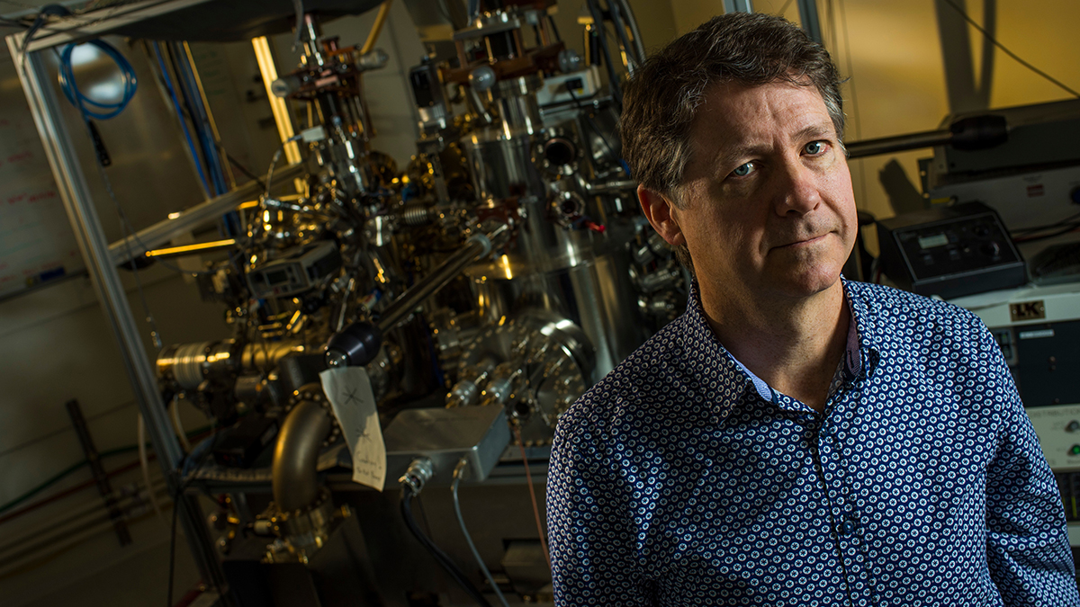
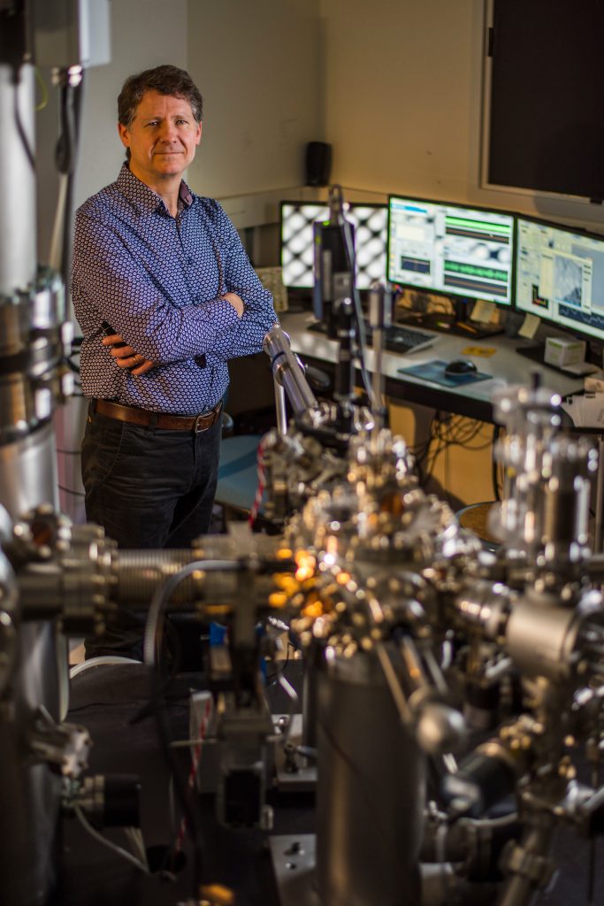
Atomic-scale manufacturing relies on scanning probe microscopy, which can take images to the trillionths of a metre, study a molecule’s fundamental magnetic or electronic properties, or modify atoms like silicon. However, the probe’s needle-like tip consists of a single metal atom, which easily degrades into an imprecise “double-tip” after interacting with only a few atoms. Normally the probe is sharpened manually, but in a paper published last May in ACS Nano, an American nanoscience journal, post-doctoral fellow Moe Rashidi, and Professor Robert Wolkow detailed their success at AI-assisted sharpening.
“I was just frustrated about all this process. I was spending two hours in the lab just doing this thing: sharpening. I just thought, ‘yeah, why not, we should automate it,’” Rashidi said. “After applying [AI], I saw that I got a very high accuracy at 97 per cent”
Rashidi said repairing the probe manually is a random and inconsistent process, so he and Wolkow automated it by teaching an AI to distinguish between a good and bad tip.
“You make ten atoms, the probe gets bad, you go there, sharpen it, come back, make another ten atoms, and the probe gets bad,” Rashidi said. “So most of our time we spend to sharpen this probe.”
Rashidi is optimistic that AI-assisted automated probe sharpening will become prevalent in a few years so that his fellow scientists can focus their time on productive tasks like reading papers, writing, or experimenting.
Rashidi’s next goal is to use AI to automate the processes around the patterning of atoms as there currently is no method to ensure it is precise. He referred to some of his earlier research they were able to modify silicon atoms in a pattern to transfer and store information at a much higher density than complementary metal-oxide-semiconductor technology (CMOS), which is found in the circuitry of most electronics.
“Right now with CMOS, they are almost at the end; the gates’ length is like fourteen nanometers and they cannot go smaller than that. They have to find another way to make electronics faster and cheaper,” Rashidi said.
Ultimately, he hopes atomic-scale manufacturing can lead to technology that surpasses CMOS, especially in terms of energy efficiency.
“If we can overcome this patterning issue, it could be huge,” Rashidi said. “In order to make that technology, we need to automate everything. We need all these pieces together to automate the process.”